Shanxi AoYuDa New Materials Co., Ltd
Service hotline:+86 15191788646
+86 0917-3336577


+86 18292768861
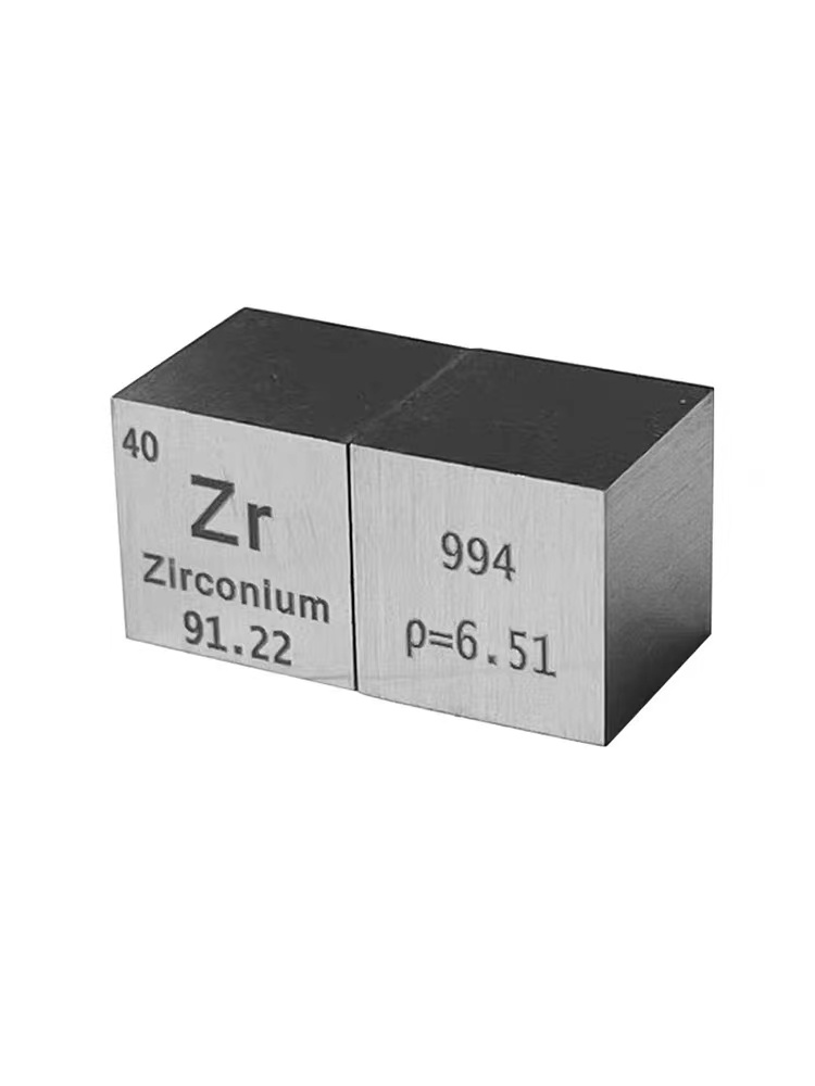
Zirconium target
Coating target is a kind of sputtering source to form various functional films on the substrate by magnetron sputtering, multi arc ion plating or other types of coating system under appropriate process conditions. In short, the target material is the target material bombarded by high-speed charged particles. When it is used in high-energy laser weapons, different power densities, different output waveforms and different wavelengths of laser interact with different targets, different damage effects will be produced. For example: evaporation magnetron sputtering coating is heating evaporation coating, aluminum film, etc. By replacing different targets (such as aluminum, copper, stainless steel, titanium, nickel targets, etc.), different film systems (such as super hard, wear-resistant, anti-corrosion alloy films, etc.) can be obtained.
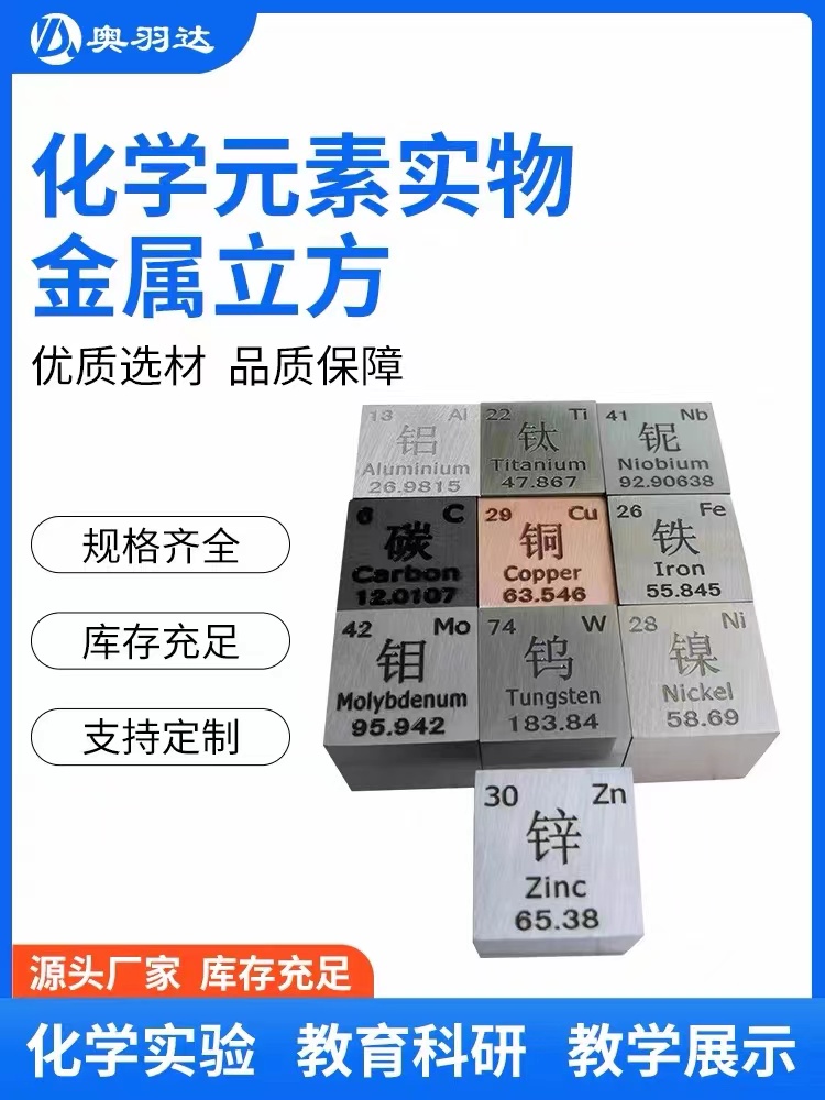
Material classification
Metal target
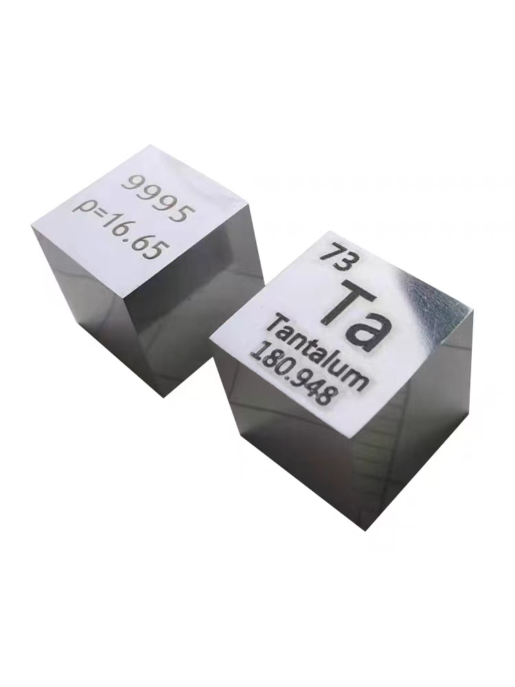
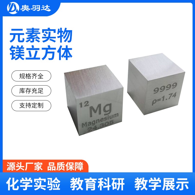
Ni, Ti, Zn, Cr, Mg, Nb, Sn, Al, in, Fe, Fe, Zr Al, Ti Al, Zr, Al, Zr, Al, Al, Al, Al, Fe, Zr, Zr, Al Si, Si, Cu, Cu, Cu, Cu, Ta, GE, Ag, Ag, Co, Au, Gd target Gd, La target La, YTY target, CE target CE, stainless steel, stainless steel target, Ni Cr target niccr, Ni Cr target, Ni Cr target, haftarget HF, haftarget HF, Mo, Mo, Mo, Mo, Mo, Mo, Mo, Mo, Mo, Mo, Mo, Fe target Mo, Fe target Mo, Fe target Mo, Fe target Mo, Fe target, Fe target, Al target Al Si, Si, Si, Cu, Cu, Cu, Ta, Ge target Ge, Ag, Ag, Co, Au, Gd target Gd, La target La, ytnickel Target FeNi, tungsten target, W, etc.
Ceramic target
ITO target, magnesium oxide target, iron oxide target, silicon nitride target, silicon carbide target, titanium nitride target, chromium oxide target, zinc oxide target, zinc sulfide target, silica target, silicon dioxide target, cerium oxide target, zirconia target, niobium pentoxy target, titanium dioxide target, zirconia target, hafnium dioxide target, titanium dioxide target, zirconium diboride target, tungsten triode target, aluminum oxide target Tantalum pentoxy, niobium oxide, magnesium fluoride, yttrium fluoride, zinc selenite, aluminum nitride, silicon nitride, boron nitride, titanium nitride, silicon carbide, lithium niobate, PR titanate, barium titanate, lanthanum titanate, nickel oxide, sputtering target, etc.
Alloy target
The target of Fe Co, Al Si, ti si, CRSI, ZnAl, tizn, Ti Al, Ti Zr, ti si, Ni, Ni, Ni Cr, NiAl, NIV and NiFe are also discussed.
Production technology
Magnetron sputtering target
1) Magnetron sputtering principle:
An orthogonal magnetic field and electric field are added between the target electrode (cathode) and anode to fill the required inert gas (usually Ar gas) in the high vacuum chamber. The permanent magnet forms a 250-350 Gauss magnetic field on the surface of the target material, and the orthogonal electromagnetic field is formed with the high voltage electric field. Under the action of electric field, Ar gas ionizes into positive ions and electrons. A certain negative high pressure is added to the target. The electron from the target pole is affected by the magnetic field and the ionization probability of working gas increases. A high density plasma is formed near the cathode. Ar ions accelerate to the target surface under the action of Lorentz force, bombard the target surface at a high speed, so that the atoms sputtering on the target follow the target Momentum conversion principle is used to deposit film by moving away from target surface with high kinetic energy. Magnetron sputtering is generally divided into two types: DC sputtering and RF sputtering. The principle of DC sputtering equipment is simple, and the rate is also fast when sputtering metal. The RF sputtering is widely used. Besides sputtering conductive materials, non-conductive materials can be sputtered, and reactive sputtering can also be used to prepare oxide, nitride and carbide. If RF frequency is increased, it will become microwave plasma sputtering. Nowadays, ECR type microwave plasma sputtering is commonly used.
2) Magnetron sputtering target type:
Metal sputtering target, alloy sputtering coating target, ceramic sputtering coating target, boride ceramic sputtering target, carbide ceramic sputtering target, fluoride ceramic sputtering target, nitride ceramic sputtering target, oxide ceramic target, selenide ceramic sputtering target, silicide ceramic sputtering target, sulfide ceramic sputtering target, tellurite ceramic sputtering target, and its He is a ceramic target, a CR SiO 2 ceramic target, an InP, a lead arsenide target (pbas), an indium arsenide target (InAs).
application area
As we all know, the development trend of target material technology is closely related to the film technology development trend of downstream application industry. With the improvement of application industry in film products or components, target technology should also change accordingly. For example, IC manufacturer has been committed to the development of low resistivity copper wiring in recent years, and it is expected that the original aluminum film will be replaced by a large margin in the next few years. Therefore, it is urgent to develop copper target and its required barrier target. In addition, in recent years, FPD has replaced the computer display and television market which was mainly CRT, which will also greatly increase the technical and market demand of ITO target. In addition, in terms of storage technology. The demand for high density, high capacity hard disk and high density erasable disc is increasing continuously, which all lead to the change of the demand of application industry for target materials. The main application fields of target materials and the development trend of target materials in these fields will be introduced.
Microelectronics
In all applications, the semiconductor industry has the most stringent requirements for the quality of target sputtering film. Today 12 inch (300) silicon chips have been made, while the width of the interconnect is decreasing. The requirements of silicon wafer manufacturers for target materials are large size, high purity, low segregation and fine grain, which requires the target made with better microstructure. The diameter and uniformity of the crystal particles of the target have been considered to be the key factors affecting the deposition rate of the films. In addition, the purity of the film has a great relationship with the purity of the target. The copper target with 99.995% (4n5) purity in the past may meet the needs of semiconductor manufacturer 0.35pm process, but it can not meet the current process requirements of 0.25um, while the 0.18um} technology of less than m or even 0.13M process will require the target purity to reach 5 or more than 6N. Compared with aluminum, copper has higher resistance to electric migration and lower resistivity, which can meet the requirements! The need of conducting wire routing under 0.25um is required but it has other problems: copper and organic medium materials have low adhesion strength, and are prone to react, which leads to the corrosion of copper interconnects of chips and open circuit. In order to solve these problems, a barrier layer is needed between copper and dielectric layer. The barrier materials generally use metals and compounds with high melting point and high resistivity. Therefore, the thickness of barrier layer is less than 50nm, and the adhesion property with copper and dielectric materials is good. The barrier materials of copper and aluminum are different. New target materials need to be developed. The barrier layer of copper interconnection uses target materials including TA, W, TASI, WSI, etc. but TA and W are refractory metals. It is relatively difficult to make. Currently, the research on the replacement materials of molybdenum and chromium is being carried out.
For display
FPD has been impacting the market of computer display and television mainly based on CRT in recent years, and will also drive the technical and market demand of ITO target. There are two ITO targets nowadays. One is to mix indium oxide and tin oxide powder in nano state and then sintering, and the other is to use indium tin alloy target. ITO thin films can be made by direct current reactive sputtering, but the surface of indium tin alloy can be oxidized and the sputtering rate is affected, and it is difficult to obtain large-scale target. Nowadays, the first method is generally used to produce ITO target. It is deposited rapidly by l} IRF reactive sputtering. It can accurately control the thickness of film, high conductivity, good consistency of film, and strong adhesion with substrate. But the target is difficult to make because indium oxide and tin oxide are not easy to sintering together. Generally, ZrO2, Bi2O3, CEO and other sintering additives can obtain 93% - 98% target with theoretical density. The properties of ITO films formed by this method have great relationship with additives. The Japanese scientists use bizo as additive, Bi2O3 melts at 820cr, and the sintering temperature exceeds the part at L500 ℃ has evaporated, so that the pure ITO target can be obtained under the liquid sintering condition. The required oxide raw materials are not necessarily nanoparticles, which can simplify the previous process. The tunning resistance of ITO films obtained by using such target materials is 8.1 × 10n-cm, which is close to the resistivity of pure ITO films. FPD and conductive glass are of considerable size, and the width of conductive glass can reach 3133_ In order to improve the utilization of target, ITO target of different shapes, such as cylindrical, is developed. In 2000, the National Development Planning Commission and the Ministry of science and technology included ITO large targets in the guide to key areas of information industry with priority development at present.
For storage
In storage technology, the development of high density and large capacity hard disk requires a large number of giant magnetoresistance film materials. The COF Cu multilayer composite film is a widely used giant magnetoresistance film structure. TbFeCo alloy target material needed by magnetic disc is still developing. The magnetic disc made with it has the characteristics of large storage capacity, long life and repeated non-contact erasure. The magneto-optical disk developed today has the layer composite membrane structure of tbfeco/ta and tbfeco/al. The Kerr rotation angle of tbfeco/ai structure reaches 58, while tbfecofcoffa can be close to 0.8. It is found that the target with low permeability has high AC PD voltage l anti electric strength.
PCM based on germanium antimony telluride has shown significant commercial potential, which is an alternative memory technology in NOR flash memory and some DRAM markets. However, one of the challenges in realizing a faster and proportionate reduction is the lack of fully closed units that can further reduce the reset current. Reducing reset current can reduce the power consumption of memory, prolong battery life and improve data bandwidth. This is very important for the current data centric and highly portable consumer equipment.
Hotline
+86 18292768861 中文版
中文版 English